Compatible J-Link OB ARM Simulation Download Debugger
- Simple design but effective target board debugging
- Compatible with most SCMs with an SWD interface
- Support most MUC manufacturers
- Easy connection with only 4 pins needed
- Has same function with an original J-Link-OB
Introduction
It’s usually designed for big companies’ evaluation boards (" onboard "), and that is why it’s named with an "OB" suffix. The debugger can interchange data with PC through the USB port, and on the other side to communicate with a supportive device by SWD/JTAG to accomplish debugging simulation download tasks. The ARM OB simulation debugger has no JTAG interface comparing with the original OB debugger, but only the SWD interface left to cope with ARM-based MCU debugging download.
Supported Core
Any Single Chip Micyoco (SCM) with an SWD interface includes ARM7911, Cortex-M0/M1/M2/ M3/M4/A5/-A8/A9, and etc.
Supported MUC Manufacturers
ST Microelectronics (ST), Freecale, Nuvoton, NXP, TI, Cypress, Atmel, Analog, Fujitsu, Toshiba
Connecting Mode
SWD interface
Functions & Performances
Programming: programming for FLASH ROM, EEPROM, AFR, etc.
Performance: fast download with a USB2.0 interface
Simulation: support various debugging methods including full-speed, single-step, breakpoint, and etc., and view IO status, variable data, etc.
Performance: fast response with a USB2.0 interface for full speed, single-step, and breakpoint debugging
Features:
- Simplified designed with 4 test pins including VCC, SWDIO, SWCLK, and GND for high-speed download simulation
- Compatible with traditional V8 emulator and has the same functions
- Convenient to connect Android phone with a micro USB interface
- Convenient for users to debug and download target board with an output of 3.3V and max 300mA current
- Self-recovery fuse provides effective short-circuit protection and much safer debugging
- More stable performance with an ESD protection device
- Transparent heat-shrinkable tube packaging
- Stable firmware with automatic upgrade function to avoid any damage that happens while using an original V8 debugger
- Portable size just like bringing a U disk
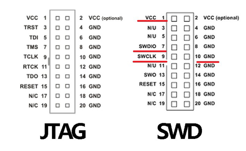
Differences between SWD & JTAG:
Compared with the JTAG interface, the SWD interface requires only 3 pins that include SWDIO, SWCLK, and GND to complete debugging and downloading simulation tasks. Thus it is more recommended.
Interface Comparison:
Usage:
This specially designed simulation download debugger is more convenient with an SWD interface compatible with the STM32 series target board and has the same functions as the original J-Link-OB.
The connections of the simulation download debugger between PC and STM series target board with an SWD interface.
Note: Do not connect the J-Link VCC port when the target board is already connected with a power supply.
The connections between the simulation download debugger between PC and a JTAG interface target board.
Notice:
If the target board is already connected with a USB power supply or others, please don’t connect the debugger’s VCC interface with the target board to avoid cross power supply. Or it will cause serious burning in the J-Link-OB debugger or the target board.
Tutorial: https://danielabalo.wordpress.com/flasear-anet-et4/